



Founded
Established January 4, 2016
2016
Since 2016, we have integrated optics, mechanics, control, software, and AI into one inspection platform optimized for PCB, substrate, and package mass-production lines.
Our in-house teams across optics, mechanics, control, software, and AI implement inspection solutions tailored to your process—fast.
Founded
Established January 4, 2016

Employees
Including Korea and India development teams

Headquarters
Pyeongtaek, Gyeonggi Province

Core products
PCB AVI, AFVI, AI, Verification System
We provide a systematic inspection platform integrating advanced AVI, AFVI, AI, and verify workflows for semiconductor substrate manufacturing.We provide a systematic inspection platform integrating advanced AVI, AFVI, AI, and verify workflows for semiconductor substrate manufacturing.

Based on ODB++ reference data generation and image processing / pattern recognition algorithms,
we design, develop, and build high-quality, high-speed machine vision inspection systems.


We provide a systematic inspection platform integrating advanced AVI, AFVI, AI, and verify workflows for semiconductor substrate manufacturing.
Based on ODB++ reference data generation and image processing / pattern recognition algorithms,
we design, develop, and build high-quality, high-speed machine vision inspection systems.

High-brightness specialty LEDs, multi-angle multi-wavelength (MAMW) illumination, and variable magnification / resolution configurations address a wide range of defect types.
ODB reference data generation, inspection condition management, history tracking, and Pixel Master operations reduce time to support new models.
Color inspection combined with high-speed parallel processing and in-house deep learning reduces overkill, missed defects, and operator burden.
High-precision X·Y·Theta axes with suction & clamping and air floating auto align structures reduce false calls from product warpage.

2016 - 2017

The stage where PIXEL launched its inspection platform by building the foundation in optics, mechanics, control, and software.
2016
After incorporation on January 4, 2016, we began developing our core inspection equipment and defined the technical direction for optics, mechanics, and control aimed at mass-production processes.
2016 - 2017
We established internal R&D through venture certification and research lab setup, and opened the India S/W development center to build a software collaboration structure.
2017 - 2020
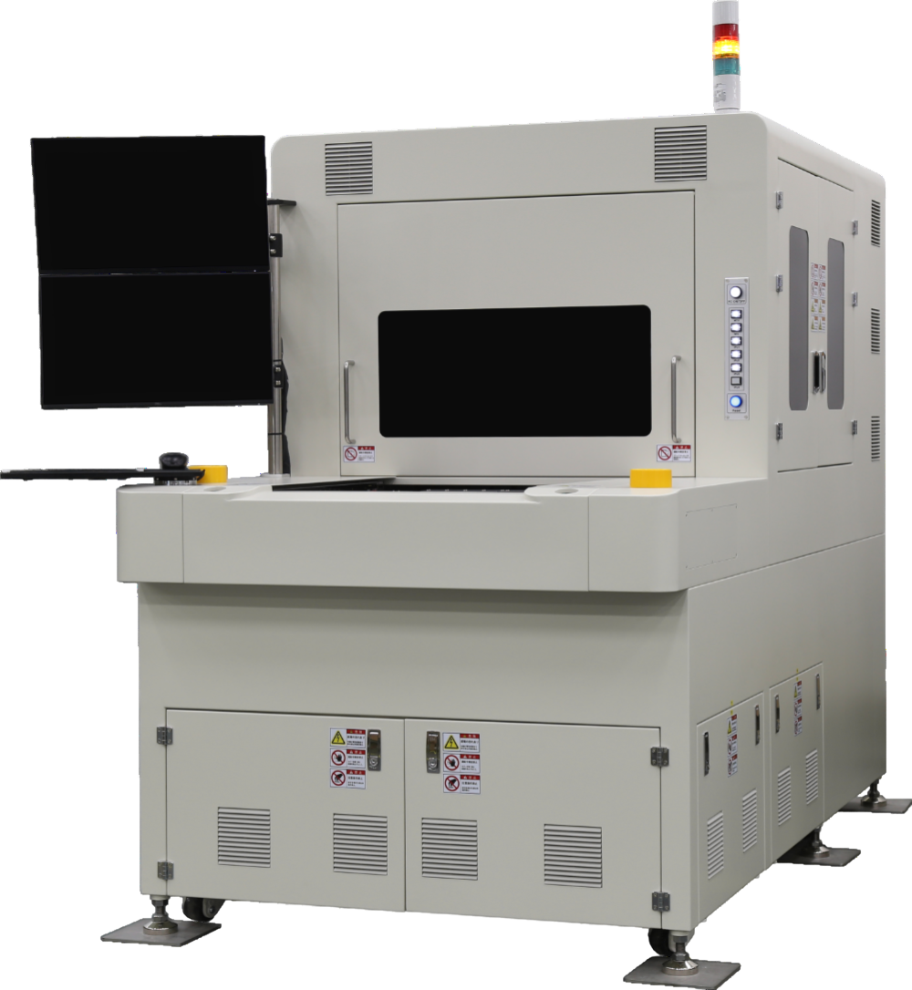
The stage where color-based AVI and AFVI were deployed on real lines, raising equipment maturity to match customer mass-production processes.
2017
We productized color-inspection-based HDI AFVI and Panel AVI and began expanding equipment configurations and coverage for customer processes.
2017 - 2020
We began first deployments on customer mass-production lines and accumulated field operating know-how, improving product maturity through equipment setup and recipe stabilization experience.
2020 - 2023
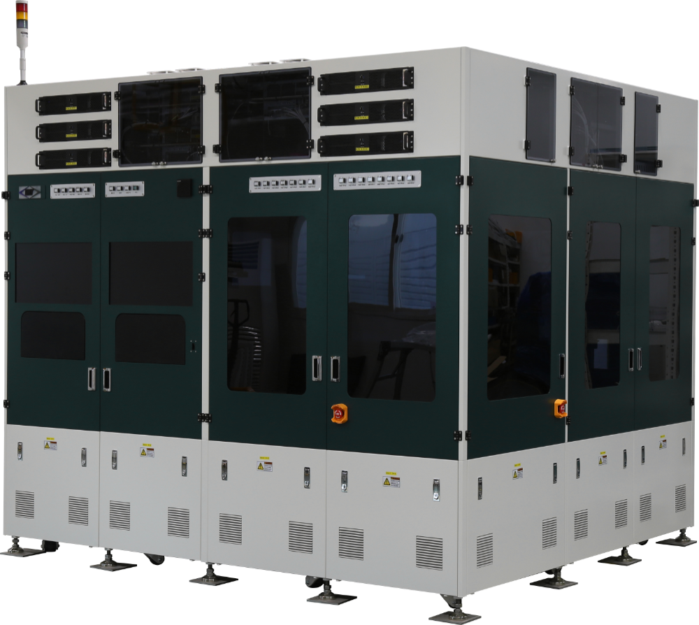
The period when relocation to Jinwi, Pyeongtaek coincided with raising quality systems, customer collaboration, and high-resolution AFVI coverage together.
2020
We relocated headquarters to Jinwi, Pyeongtaek and reorganized development, manufacturing, and customer support hubs, strengthening an operating structure that accelerates field response and equipment collaboration.
2020 - 2022
We strengthened our ISO 9001-based quality system to improve mass-production readiness and refined customer collaboration and equipment setup support.
2023
We secured Strip AFVI coverage with 1 µm-class high-resolution color and dent inspection. AI inspection and filtering advancement raised inspection operational precision.
2023 - Present
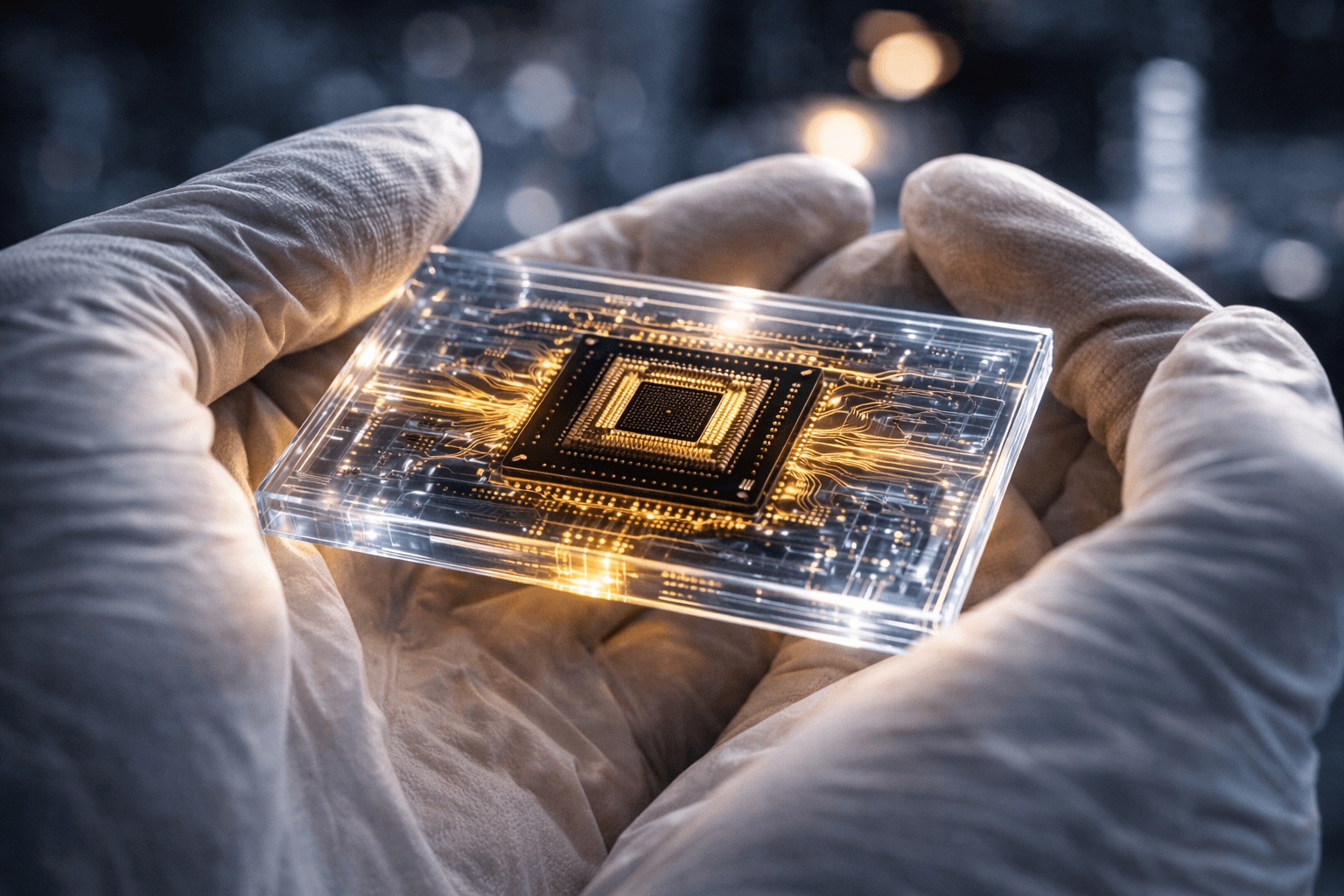
The stage of connecting AI inspection, filtering, and Verification System more precisely while broadening customer diversification and overseas reach.
2023 - Present
We are refining operational flows by improving connectivity between inspection equipment and the Verification System and linking AI inspection and filtering more deeply into field processes.
Present
We are pursuing customer diversification and expanded exports together, continuing system advancement across Panel, Strip, Tray, and Verification.
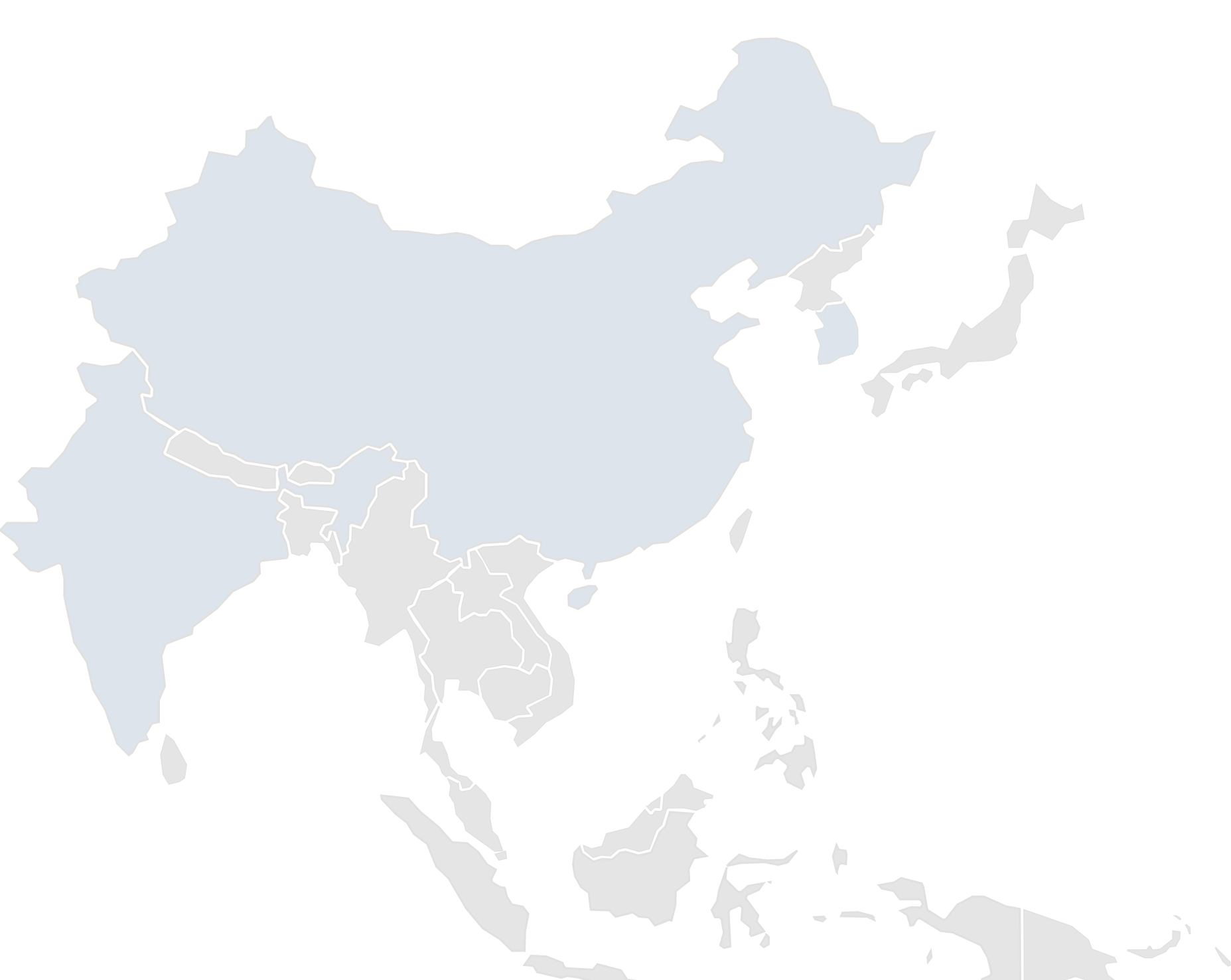

Pixel Inc.
AI-Integrated Inspection Systems
korea
india
Core hub for equipment development, manufacturing, and customer support
R&D, manufacturing, and field support connect at headquarters, where equipment demos and customer meetings take place together.
 Integrated R&D / manufacturing / field support operationsCustomer meetings and equipment demo hubKey operating node based in Pyeongtaek, Gyeonggi Province
Software development and R&D collaboration hub
The India S/W development center expands AI and inspection software capabilities and collaborates closely with Korea headquarters.
AI and inspection software developmentCollaboration structure with Korea R&D teamsKey node in the global development networkOn-site meetings, equipment demos, and sample intake reviews are scheduled in advance.We recommend confirming schedule and items to bring with your contact before visiting.Convenient access from Osan IC and Jinwi Station.